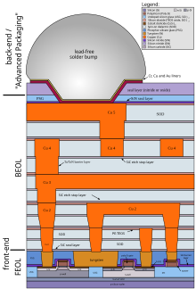
Integrated circuit
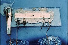
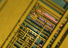
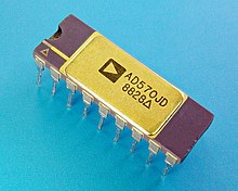
[1] Integrated circuits are used in a wide range of electronic devices, including computers, smartphones, and televisions, to perform various functions such as processing and storing information.Integrated circuits are orders of magnitude smaller, faster, and less expensive than those constructed of discrete components, allowing a large transistor count.The choice of terminology frequently appears in discussions related to whether Moore's Law is obsolete.An early attempt at combining several components in one device (like modern ICs) was the Loewe 3NF vacuum tube first made in 1926.Between 1953 and 1957, Sidney Darlington and Yasuo Tarui (Electrotechnical Laboratory) proposed similar chip designs where several transistors could share a common active area, but there was no electrical isolation to separate them from each other.[11] The monolithic integrated circuit chip was enabled by the inventions of the planar process by Jean Hoerni and p–n junction isolation by Kurt Lehovec.[18][19][20][21][22] A precursor idea to the IC was to create small ceramic substrates (so-called micromodules),[23] each containing a single miniaturized component.This idea, which seemed very promising in 1957, was proposed to the US Army by Jack Kilby[23] and led to the short-lived Micromodule Program (similar to 1951's Project Tinkertoy).[26] In his patent application of 6 February 1959,[27] Kilby described his new device as "a body of semiconductor material … wherein all the components of the electronic circuit are completely integrated".[30] However, Kilby's invention was not a true monolithic integrated circuit chip since it had external gold-wire connections, which would have made it difficult to mass-produce.Computers such as IBM 360 mainframes, PDP-11 minicomputers and the desktop Datapoint 2200 were built from bipolar integrated circuits,[35] either TTL or the even faster emitter-coupled logic (ECL).Following the development of the self-aligned gate (silicon-gate) MOSFET by Robert Kerwin, Donald Klein and John Sarace at Bell Labs in 1967,[52] the first silicon-gate MOS IC technology with self-aligned gates, the basis of all modern CMOS integrated circuits, was developed at Fairchild Semiconductor by Federico Faggin in 1968.[35] Advances in IC technology, primarily smaller features and larger chips, have allowed the number of MOS transistors in an integrated circuit to double every two years, a trend known as Moore's law.[56] Because speed, capacity, and power consumption gains are apparent to the end user, there is fierce competition among the manufacturers to use finer geometries.[58] The expected shrinking of feature sizes and the needed progress in related areas was forecast for many years by the International Technology Roadmap for Semiconductors (ITRS).As of 2018[update], the vast majority of all transistors are MOSFETs fabricated in a single layer on one side of a chip of silicon in a flat two-dimensional planar process.Researchers have produced prototypes of several promising alternatives, such as: As it becomes more difficult to manufacture ever smaller transistors, companies are using multi-chip modules/chiplets, three-dimensional integrated circuits, package on package, High Bandwidth Memory and through-silicon vias with die stacking to increase performance and reduce size, without having to reduce the size of the transistors.Some of the latest EDA tools use artificial intelligence (AI) to help engineers save time and improve chip performance.The small size of these circuits allows high speed, low power dissipation, and reduced manufacturing cost compared with board-level integration.[86] Modern electronic component distributors often further sub-categorize integrated circuits: The semiconductors of the periodic table of the chemical elements were identified as the most likely materials for a solid-state vacuum tube.Today, monocrystalline silicon is the main substrate used for ICs although some III-V compounds of the periodic table such as gallium arsenide are used for specialized applications like LEDs, lasers, solar cells and the highest-speed integrated circuits.Photolithography is used to mark different areas of the substrate to be doped or to have polysilicon, insulators or metal (typically aluminium or copper) tracks deposited on them.The earliest integrated circuits were packaged in ceramic flat packs, which continued to be used by the military for their reliability and small size for many years.Extremely small surface-mount technology parts often bear only a number used in a manufacturer's lookup table to find the integrated circuit's characteristics.National laws protecting IC layout designs have been adopted in a number of countries, including Japan,[98] the EC,[99] the UK, Australia, and Korea.[51] Further development, driven by the same MOSFET scaling technology and economic factors, led to "large-scale integration" (LSI) by the mid-1970s, with tens of thousands of transistors per chip.True LSI circuits, approaching 10,000 transistors, began to be produced around 1974, for computer main memories and second-generation microprocessors.The complexity and density of modern VLSI devices made it no longer feasible to check the masks or do the original design by hand.[122] Further, signal sources and destinations are physically closer on die, reducing the length of wiring and therefore latency, transmission power costs and waste heat from communication between modules on the same chip.This has led to an exploration of so-called Network-on-Chip (NoC) devices, which apply system-on-chip design methodologies to digital communication networks as opposed to traditional bus architectures.These artistic additions, often created with great attention to detail, showcase the designers' creativity and add a touch of personality to otherwise utilitarian components.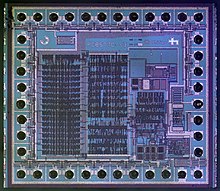


Silicon ChipMicrochip (disambiguation)pinoutselectronic circuitselectronic componentstransistorsresistorscapacitorssemiconductorsiliconcomputerssmartphonestelevisionselectronicstransistor countmass productionintegrated circuit designhome appliancescomputer processorsmicrocontrollersVery-large-scale integrationsemiconductor device fabricationMoore's lawphotolithographyhigh production volumes2.5D ICthin-film transistorsthick-film technologieshybrid integrated circuitsJack KilbygermaniumLoewe 3NFtax avoidanceamplifierdiscrete componentsWerner JacobiSiemens AGhearing aidsGeoffrey DummerRoyal Radar EstablishmentMinistry of DefenceWashington, D.C.Sidney DarlingtonElectrotechnical Laboratoryelectrical isolationplanar processJean Hoernip–n junction isolationKurt LehovecInvention of the integrated circuitSurface passivationRobert NoyceTexas InstrumentsUS Air ForceNobel PrizeFairchild SemiconductorTransistor–transistor logicJames L. BuieTRW Inc.Dov Frohmanprocessorsminicomputersmainframe computersIBM 360PDP-11Datapoint 2200bipolaremitter-coupled logicList of semiconductor scale examplesMixed-signal integrated circuitThree-dimensional integrated circuitVery Large Scale Integrationmetal–oxide–semiconductorMOSFETshigh-density integrated circuitsbipolar transistorslist of IEEE milestonesGeneral Microelectronicsshift registertransistor densitylarge-scale integrationself-aligned gateDonald Kleinsilicon-gateself-aligned gatesFederico Faggincomputingmicroprocessorscomputer processormicrocontrollervery large-scale integrationaerospacepocket calculatorsIntel 8008smaller featuresthe numberMOS transistorsswitching power consumptionmemory capacityDennard scalingMOSFET scalingmicronsnanometersmillimetersInternational Technology Roadmap for SemiconductorsInternational Roadmap for Devices and SystemsCharge-coupled devicesactive-pixel sensorsphotographic filmmicroelectromechanical systemsDLP projectorsinkjet printersaccelerometersMEMS gyroscopesairbagsoptical computingPhotonic integrated circuitsphotonicssensormedical implantsbioelectroniccorrosionbiodegradationthrough-silicon viagraphene transistorscarbon nanotube field-effect transistor