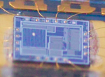
Photodiode
Photodiodes are used in a wide range of applications throughout the electromagnetic spectrum from visible light photocells to gamma ray spectrometers.If the circuit is opened or has a load impedance, restricting the photocurrent out of the device, a voltage builds up in the direction that forward biases the diode, that is, anode positive with respect to cathode.For optimum power output, the photovoltaic cell will be operated at a voltage that causes only a small forward current compared to the photocurrent.[4] The leakage current of a good PIN diode is so low (<1 nA) that the Johnson–Nyquist noise of the load resistance in a typical circuit often dominates.This allows each photo-generated carrier to be multiplied by avalanche breakdown, resulting in internal gain within the photodiode, which increases the effective responsivity of the device.The novel concept is a two-in-one power source plus transistor device that runs on solar energy by exploiting a memresistive effect in the flow of photogenerated carriers.Semiconductor devices such as diodes, transistors and ICs contain p–n junctions, and will not function correctly if they are illuminated by unwanted light.If these housings are not completely opaque to high-energy radiation (ultraviolet, X-rays, gamma rays), diodes, transistors and ICs can malfunction[13] due to induced photo-currents.A photodiode is often combined into a single component with an emitter of light, usually a light-emitting diode (LED), either to detect the presence of a mechanical obstruction to the beam (slotted optical switch) or to couple two digital or analog circuits while maintaining extremely high electrical isolation between them, often for safety (optocoupler).They are also widely used in various medical applications, such as detectors for computed tomography (coupled with scintillators), instruments to analyze samples (immunoassay), and pulse oximeters.Instead, if high sensitivity is needed, avalanche photodiodes, intensified charge-coupled devices or photomultiplier tubes are used for applications such as astronomy, spectroscopy, night vision equipment and laser rangefinding.The PPD (usually PNP) is used in CMOS active-pixel sensors; a precursor NPNP triple junction variant with the MOS buffer capacitor and the back-light illumination scheme with complete charge transfer and no image lag was invented by Sony in 1975.In some applications, photodiode arrays allow for high-speed parallel readout, as opposed to integrating scanning electronics as in a charge-coupled device (CCD) or CMOS sensor.


PassivecurrentcathodeElectronic symbolphotonX-raysgamma rayssolar cellsPIN structurep–n junctionelectronphotoelectric effectdepletion regionphotocurrentirradianceload linesphotovoltaic effectcapacitancedark currentJohnson–Nyquist noiseAvalanche photodiodesavalanche breakdownbipolar transistorjunctionJohn N. ShiveresponsivitysolaristorphotonselectronsbandgapElectromagnetic spectrumwavelengthSiliconGermaniumIndium gallium arsenideLead(II) sulfideMercury cadmium tellurideRadiation hardeningenergy harvestingSpectral responsivityquantum efficiencycalibrationResponse timeRamo's theoremintegralRC time constantimpulse responseNoise-equivalent powerspecific detectivitysensitivitybit error ratephotodetectorsphotoconductorscharge-coupled devicesphotomultiplierconsumer electronicscompact discsmoke detectorsremote control devicestelevisionscameralight-emitting diodeslotted optical switchcoupleisolationoptocouplersensoroptical absorbancecomputed tomographyscintillatorsimmunoassaypulse oximetersPIN diodesoptical communicationsintensified charge-coupled devicesastronomyspectroscopynight vision equipmentlaser rangefindingphotomultiplierswavelengthssemiconductor materialsPIN photodiodebipolar junction transistoractive-pixel sensorsimage sensorsshutter lagNobukazu Teranishiconsumer electronicvideo camerasdigital still camerasoptical mouseoptical micecharge-coupled deviceCMOS sensorpassive-pixel sensoractive-pixel sensoramplificationMOSFETcapacitortransistorsfabricatemicrolithographyElectronicsBand gapInfraredOptoelectronicsOptical interconnectLight PeakInterconnect bottleneckOptical fiber cableOptical communicationParallel optical interfaceOpto-isolatorSemiconductor deviceSolar cellAvalanche photodiodeTransducerLEDs as photodiode light sensorsLight meterImage sensorTransimpedance amplifierPhotoelectric sensorpublic domain materialGeneral Services AdministrationRiordan, Michael