Laser diode
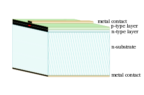
The choice of the semiconductor material determines the wavelength of the emitted beam, which in today's laser diodes range from the infrared (IR) to the ultraviolet (UV) spectra.Forward electrical bias across the laser diode causes the two species of charge carrier – holes and electrons – to be injected from opposite sides of the PIN junction into the depletion region.(A depletion region, devoid of any charge carriers, forms as a result of the difference in electrical potential between n- and p-type semiconductors wherever they are in physical contact.)(In a conventional semiconductor junction diode, the energy released from the recombination of electrons and holes is carried away as phonons (lattice vibrations) rather than as photons.)The properties of silicon and germanium, which are single-element semiconductors, have bandgaps that do not align in the way needed to allow photon emission and are not considered direct.Other materials, the so-called compound semiconductors, have virtually identical crystalline structures as silicon or germanium but use alternating arrangements of two different atomic species in a checkerboard-like pattern to break the symmetry.In the simplest form of laser diode, an optical waveguide is made on that crystal's surface, such that the light is confined to a relatively narrow line.The width of the gain curve will determine the number of additional side modes that may also lase, depending on the operating conditions.For single-spatial-mode lasers, using symmetrical lenses, the collimated beam ends up being elliptical in shape, due to the difference in the vertical and lateral divergences.Bernard, G. Duraffourg, and William P. Dumke in the early 1960s, coherent light emission from a gallium arsenide (GaAs) semiconductor diode (a laser diode) was demonstrated in 1962 by two US groups led by Robert N. Hall at the General Electric research center[5] and by Marshall Nathan at the IBM T.J. Watson Research Center.[7] It was initially speculated, by MIT's Ben Lax among other leading physicists, that silicon or germanium could be used to create a lasing effect, but theoretical analyses convinced William P. Dumke that these materials would not work.The dominant challenge for the remainder of the 1960s was to obtain low threshold current density at 300 K and thereby to demonstrate continuous-wave lasing at room temperature from a diode laser.Heterojunctions (formed from heterostructures) had been recognized by Herbert Kroemer, while working at RCA Laboratories in the mid-1950s, as having unique advantages for several types of electronic and optoelectronic devices, including diode lasers.An admixture of aluminum replaced gallium in the semiconductor crystal and raised the bandgap of the p-type injector over that of the n-type layers beneath.The first laser diode to achieve continuous-wave operation was a double heterostructure demonstrated in 1970 essentially simultaneously by Zhores Alferov and collaborators (including Dmitri Z. Garbuzov) of the Soviet Union, and Morton Panish and Izuo Hayashi working in the United States.The advantage of a DH laser is that the region where free electrons and holes exist simultaneously—the active region—is confined to the thin middle layer.The problem with the simple quantum well diode described above is that the thin layer is simply too small to effectively confine the light.This grating acts like an optical filter, causing a single wavelength to be fed back to the gain region and lase.Several techniques have been proposed in order to enhance the single-mode operation in these kinds of lasers by inserting a one-phase-shift (1PS) or multiple-phase-shift (MPS) in the uniform Bragg grating.[12] However, multiple-phase-shift DFB lasers represent the optimal solution because they have the combination of higher side-mode suppression ratio and reduced spatial hole-burning.The active region length is very short compared with the lateral dimensions so that the radiation emerges from the surface of the cavity rather than from its edge as shown in the figure.In contrast, a conventional in-plane semiconductor laser entails light propagation over distances of from 250 μm upward to 2 mm or longer.The significance of the short propagation distance is that it causes the effect of antiguiding nonlinearities in the diode laser gain region to be minimized.Several workers demonstrated optically pumped VECSELs, and they continue to be developed for many applications, including high-power sources for use in industrial machining (cutting, punching, etc.)CEO Donald Scifres and CTO David Welch presented new reliability performance data at, e.g., SPIE Photonics West conferences of the era.In the mid-1990s, IBM Research - Ruschlikon, Switzerland announced that it had devised its so-called E2 process, which conferred extraordinary resistance to the COD in GaAs-based lasers.Diode lasers can be used in a great many fields; since light has many different properties (power, wavelength, spectral and beam quality, polarization, etc.[19][20][21][22][23][24] The shrinking size and cost[25] of the units and their increasing user-friendliness makes them very attractive to clinicians for minor soft-tissue procedures.Laser diodes are used for their narrow spectral properties in the areas of range-finding, telecommunications, infra-red countermeasures, spectroscopic sensing, generation of radio-frequency or terahertz waves, atomic clock state preparation, quantum key cryptography, frequency doubling and conversion, water purification (in the UV), and photodynamic therapy (where a particular wavelength of light would cause a substance such as porphyrin to become chemically active as an anti-cancer agent only where the tissue is illuminated by light).Areas of use include clock distribution for high-performance integrated circuits, high-peak-power sources for laser-induced breakdown spectroscopy sensing, arbitrary waveform generation for radio-frequency waves, photonic sampling for analog-to-digital conversion, and optical code-division-multiple-access systems for secure communication.


semiconductorlight-emitting diodecarrier generation and recombinationRobert N. HallNick Holonyak, Jr.cathodescanning electron microscopelasingjunctionrecombinationinfraredultravioletfiber-optic communicationsbarcode readerslaser pointersBlu-raylaser printinglaser scanninglight beamPIN diodedirect band-gapepitaxialcrystal growthcladdingquantum wellscharge carrierelectronsdepletion regionsolid-state lasersoptical pumpingrecombinespontaneous emissionphononslasing thresholddirect bandgapsilicongermaniumGallium arsenideindium phosphidegallium antimonidegallium nitridestimulated emissionpolarizationindirect bandgapoptical cavityFabry–Pérottransverse optical modesdiffraction-limitedpumpingdiffractioncollimated beamlaser pointerNick HolonyakcoherentGeneral ElectricIBM T.J. Watson Research CenterYorktown Heightsgallium arsenide phosphideMIT Lincoln LaboratoryTexas InstrumentsRCA LaboratoriesSoviet UnionNikolay Basovepitaxyheterojunctionmolecular-beam epitaxychemical vapor depositionaluminum gallium arseniderefractive indexHerbert Kroemerdouble heterostructurecontinuous-waveZhores AlferovDmitri Z. GarbuzovMorton PanishIzuo Hayashi2000 Nobel Prize in Physicsbandgapaluminium gallium arsenideheterostructureactive regionQuantum well laserquantum wellwavefunctiondensity of stateswaveguidequantum wirequantum dotsQuantum cascade laserwavelengthsInterband cascade laserdistributed Bragg reflector laserdiffraction gratingVCSELsDistributed-feedback laseranti-reflection coatedVertical-cavity surface-emitting laserVertical-cavity surface-emitting lasersdielectric mirrorsVertical-external-cavity surface-emitting-laserVECSELsepitaxiallyfrequency doublingtunable lasersreliabilityfailure issueslight-emitting diodescatastrophic optical damageReverse engineeringcleavingspecularly reflectingcrystallographic planeSurface statesphononelectronthermal runawaypositive feedbacktelecommunicationsDavid Sarnoff Research CenterPrinceton, New Jerseyaluminum oxideanti-reflective coatingSwitzerlandinertial confinement fusionfiber-opticrangefinders