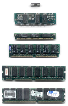
Semiconductor memory
[5] The memory storage capacity for M number of address lines is given by 2M, which is usually in power of two: 2, 4, 8, 16, 32, 64, 128, 256 and 512 and measured in kilobits, megabits, gigabits or terabits, etc.By combining several integrated circuits, memory can be arranged into a larger word length and/or address space than what is offered by each chip, often but not necessarily a power of two.To increase data rate, in some of the latest types of memory chips such as DDR SDRAM multiple words are accessed with each read or write operation.[9] Bipolar semiconductor memory made from discrete devices was first shipped by Texas Instruments to the United States Air Force in 1961.The same year, the concept of solid-state memory on an integrated circuit (IC) chip was proposed by applications engineer Bob Norman at Fairchild Semiconductor.[15] This led to MOSFETs eventually replacing magnetic cores as the standard storage elements in computer memory.Wood and R. Ball of the Royal Radar Establishment proposed digital storage systems that use CMOS (complementary MOS) memory cells, in addition to MOSFET power devices for the power supply, switched cross-coupling, switches and delay-line storage.[21] In 1967, Dennard filed a patent under IBM for a single-transistor DRAM memory cell, based on MOS technology.[31][32] In 1967, Dawon Kahng and Simon Sze of Bell Labs proposed that the floating gate of a MOS semiconductor device could be used for the cell of a reprogrammable read-only memory (ROM), which led to Dov Frohman of Intel inventing EPROM (erasable PROM) in 1971.[33] EEPROM (electrically erasable PROM) was developed by Yasuo Tarui, Yutaka Hayashi and Kiyoko Naga at Japan's Ministry of International Trade and Industry (MITI) Electrotechnical Laboratory in 1972.

Computer memorydata storageMemory cellMemory coherenceCache coherenceMemory hierarchyMemory access patternMemory mapfloating-gateContinuous availabilityAreal density (computer storage)Block (data storage)Object storageDirect-attached storageNetwork-attached storageStorage area networkBlock-level storageSingle-instance storageStructured dataUnstructured dataBig dataMetadataData compressionData corruptionData cleansingData degradationData integrityData securityData validationData validation and reconciliationData recoveryStorageData clusterDirectoryShared resourceFile sharingFile systemClustered file systemDistributed file system for cloudDistributed data storeDistributed databaseDatabaseData bankData storeData deduplicationData structureData redundancyReplication (computing)Memory refreshStorage recordInformation repositoryKnowledge baseComputer fileObject fileFile deletionFile copyingBackupCore dumpHex dumpData communicationInformation transferTemporary fileCopy protectionDigital rights managementVolume (computing)Boot sectorMaster boot recordVolume boot recordDisk arrayDisk imageDisk mirroringDisk aggregationDisk partitioningMemory segmentationLocality of referenceLogical diskStorage virtualizationVirtual memoryMemory-mapped fileSoftware entropySoftware rotIn-memory databaseIn-memory processingPersistence (computer science)Persistent data structureNon-RAID drive architecturesMemory pagingBank switchingGrid computingCloud computingCloud storageFog computingEdge computingDew computingAmdahl's lawMoore's lawVolatileCPU cacheScratchpad memoryQDRSRAMXDR DRAM1T-SRAMContent-addressable memoryComputational RAMDual-ported RAMVideo RAM (dual-ported DRAM)Williams–Kilburn tubeDelay-line memoryMellon optical memorySelectron tubeDekatronNon-volatileDiode matrixEEPROMROM cartridgeSolid-state storageFlash memorySolid-state driveSolid-state hybrid driveUSB flash driveIBM FlashSystemFlash Core ModuleMemory cardMemory StickCompactFlashPC Card