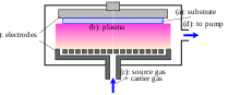
Chemical vapor deposition
Microfabrication processes widely use CVD to deposit materials in various forms, including: monocrystalline, polycrystalline, amorphous, and epitaxial.[10] Polymerization by CVD, perhaps the most versatile of all applications, allows for super-thin coatings which possess some very desirable qualities, such as lubricity, hydrophobicity and weather-resistance to name a few.[12] Recently scaled up as an integrated cleanroom process depositing large-area substrates,[13] the applications for these films are anticipated in gas sensing and low-κ dielectrics.Common source gases include silane and oxygen, dichlorosilane (SiCl2H2) and nitrous oxide[16] (N2O), or tetraethylorthosilicate (TEOS; Si(OC2H5)4).The reactions are as follows:[17] The choice of source gas depends on the thermal stability of the substrate; for instance, aluminium is sensitive to high temperature.During further process steps that occur at high temperature, the impurities may diffuse from the oxide into adjacent layers (most notably silicon) and dope them.Lower temperature deposition of silicon dioxide and doped glasses from TEOS using ozone rather than oxygen has also been explored (350 to 500 °C).Another two reactions may be used in plasma to deposit SiNH: These films have much less tensile stress, but worse electrical properties (resistivity 106 to 1015 Ω·cm, and dielectric strength 1 to 5 MV/cm).[27] The direct growth of high-quality, large single-crystalline domains of graphene on a dielectric substrate is of vital importance for applications in electronics and optoelectronics.Physical conditions such as surrounding pressure, temperature, carrier gas, and chamber material play a big role in production of graphene.Caution has to be exercised as high temperatures do pose higher danger levels in addition to greater energy costs.The study was carried out in a home-built vertical cold wall system utilizing resistive heating by passing direct current through the substrate.It provided conclusive insight into a typical surface-mediated nucleation and growth mechanism involved in two-dimensional materials grown using catalytic CVD under conditions sought out in the semiconductor industry.[32][33] In spite of graphene's exciting electronic and thermal properties, it is unsuitable as a transistor for future digital devices, due to the absence of a bandgap between the conduction and valence bands.Scaling things down, graphene nanoribbons of less than 10 nm in width do exhibit electronic bandgaps and are therefore potential candidates for digital devices.Precise control over their dimensions, and hence electronic properties, however, represents a challenging goal, and the ribbons typically possess rough edges that are detrimental to their performance.CVD can be used to produce a synthetic diamond by creating the circumstances necessary for carbon atoms in a gas to settle on a substrate in crystalline form.Diamond's very high scratch resistance and thermal conductivity, combined with a lower coefficient of thermal expansion than Pyrex glass, a coefficient of friction close to that of Teflon (polytetrafluoroethylene) and strong lipophilicity would make it a nearly ideal non-stick coating for cookware if large substrate areas could be coated economically.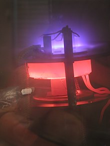


Chemical Vapor Deposition (journal)plasmacarbon nanotubesplasma-enhanced chemical vapor depositionvacuum depositionsemiconductor industrythin filmsvolatiledecomposeby-productsMicrofabricationmonocrystallinepolycrystallineamorphousepitaxialsilicondioxidecarbidenitrideoxynitridenanofibersnanotubesdiamondgraphenefluorocarbonsfilamentstungstentitanium nitridehigh-κ dielectricsphysical vapour depositionultra-high vacuumtetraethyl orthosilicatePlasma processingPlasma-enhanced CVDnanoparticleLow-energy plasma-enhanced chemical vapor depositioncrystallineAtomic layer epitaxyCombustion chemical vapor depositionnanomaterialsHybrid physical-chemical vapor depositionvaporizationMetalorganic chemical vapor depositionmetalorganicparticleLaser chemical vapor depositionatomic layer depositionGallium arsenideintegrated circuitscarbidesnitridesmetal-organic frameworkslow-κ dielectricsSiemens processPolycrystalline silicontrichlorosilanesilanenitrogenhydrogenphosphinearsinediboraneoxygendichlorosilanenitrous oxidetetraethylorthosilicatealuminiumdielectric strengthconformallythermal oxidealloyingdopingdiffusephosphorus pentoxideGlasseschlorinestressresistivitytungsten hexafluoridecopperelectroplatingtriisobutylaluminiumorganoaluminium compoundsmolybdenumtantalumtitaniumsilicidesNiobium(V) oxideniobium(V) ethoxidediethyl ethersynthetic diamondhot filamentmicrowavearc dischargesthermal conductivitycoefficient of thermal expansioncoefficient of frictionpolytetrafluoroethylenelipophilicitydopantsnanometersmicrometersmercury cadmium tellurideinfrared radiationApollo DiamondBubbler cylinderCarbonyl metallurgyElectrostatic spray assisted vapour depositionElement SixIon platingMetalorganic vapour phase epitaxyVirtual metrologyLisa McElwee-WhiteList of metal-organic chemical vapour deposition precursorsList of synthetic diamond manufacturersBibcodeNature MaterialsChemistry of MaterialsUllmann's Encyclopedia of Industrial ChemistryWayback MachineGlass transitionSupercoolingAgInSbTeBioglassBorophosphosilicate glassBorosilicate glass