PA-8000
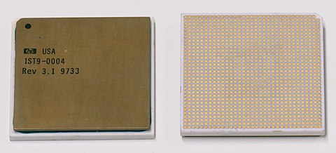
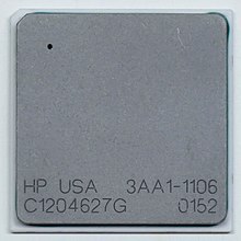
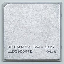
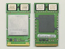
The PA-8000 (PCX-U), code-named Onyx, is a microprocessor developed and fabricated by Hewlett-Packard (HP) that implemented the PA-RISC 2.0 instruction set architecture (ISA).The PA-8000 was introduced on 2 November 1995 when shipments began to members of the Precision RISC Organization (PRO).Although the PA-8000 can execute two branch instructions per cycle, only one of the outcomes is recorded as the BHT is not dual-ported to simplify its implementation.When the same branch is encountered, and is predicted as taken, the address is sent to the instruction cache immediately, allowing the fetch to begin without delay.These bits reduce the amount of time required to decode the instruction later in the pipeline.All instructions executed in these units have a single-cycle latency and their results are written to the destination register in stage seven.The FMAC units also execute individual multiply and add instructions, which also have a latency of three cycles for both single-precision and double-precision variants.One instruction can be issued to them per clock cycle due to register port limitations, but they can operate in parallel with each other and the FMAC units.Both integer and floating-point load and store instructions are executed by two dedicated address adders.Each TLB entry can be mapped to a page with a size between 4 KB to 16 MB, in increments that are powers of four.It is packaged in a 1,085-pad flip chip alumina ceramic land grid array (LGA).[4][8] Branch prediction was improved by quadrupling the number of BHT entries to 1,024, which required the use of a two-bit algorithm in order to fit without redesign of surrounding circuitry; and by implementing a write queue that enabled two branch outcomes to be recorded by the BHT instead of one.[9] The most notable improvements are the higher operating frequencies and the on-die integration of the primary caches.[10] The higher operating frequencies and the integration of the primary caches on the same die as the core was enabled by the migration to a 0.25 μm process.[9] It was fabricated by Intel Corporation in a 0.25 μm CMOS process with five levels of aluminium interconnect.It improved the microarchitecture by using a quasi-least recently used (LRU) eviction policy for instruction cache.The PA-8700 was fabricated by IBM Microelectronics[13] in a 0.18 μm silicon on insulator (SOI) CMOS process with seven levels of copper interconnect and low-κ dielectric.The L2 cache is implemented with using four 72 Mbit (9 MB) Enhanced Memory Systems Enhanced SRAM (ESRAM) chips, which despite its name, is an implementation of 1T-SRAM – dynamic random access memory (DRAM) with a SRAM-like interface.[14] It was fabricated by IBM in 0.13 μm SOI process with copper interconnects and low-κ dielectric.The PA-8800 is packaged in a ceramic ball grid array mounted on a printed circuit board (PCB) with the four ESRAMs, forming a module similar to those used by early Itanium microprocessors.There were no microarchitecture changes, but the floating-point unit and on-die cache circuitry was redesigned to reduce power consumption, and each core subsequently dissipated approximately 35 W at 1.0 GHz.


microprocessorHewlett-PackardPA-RISC 2.0instruction set architectureHP 9000HP 3000Stratus Technologiessuperscalarout-of-orderspeculativelyprogram countertranslation lookaside bufferbranch predictionshift registerregister renamingarithmetic logic unitsfused multiply–accumulatesingle-precisiondouble-precisionRunway busphysical addressphysical memoryaluminum interconnectcomplementary metal–oxide–semiconductorflip chipalumina ceramicland grid arrayAlpha 21164Intel Corporationleast recently usedIBM Microelectronicssilicon on insulatorcopper interconnectlow-κdielectricHP 9000 Superdomedual-core1T-SRAMdynamic random access memoryfront side busItaniumcopper interconnectslow-κ dielectricprinted circuit boarddie shrinkThe RegisterMicroprocessor ReportHewlett-Packard CompanyPress ReleaseIEEE Micro