Low-energy electron microscopy
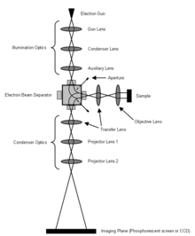
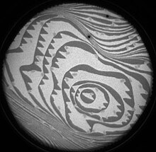
The intensity distribution of the diffraction pattern will depend on the periodicity at the sample surface and is a direct result of the wave nature of the electrons.Such phenomena include (but are not limited to): tomography, phase transitions, adsorption, reaction, segregation, thin film growth, etching, strain relief, sublimation, and magnetic microstructure.Electromagnetic quadrupole electron lenses are used, the number of which depends on how much resolution and focusing flexibility the designer wishes.The uniformity of the electrostatic field between the objective lens and specimen, limited by spherical and chromatic aberrations larger than those of any other lenses, ultimately determines the overall performance of the instrument.In most electron microscopies, the contrast aperture is introduced into the back focal plan of the objective lens (where the actual diffraction plane lies).It is worth noting that the spacing of diffracted beams does not increase with kinetic energy as for conventional LEED systems.If the surface is not homogeneous, a diffraction pattern obtained from LEED experiment appears convoluted and is therefore hard to analyze.In a microdiffraction experiment researchers may focus on a particular island, terrace, domain and so on, and retrieve a diffraction pattern composed solely of a single surface feature, making the technique extremely useful.This technique allows scientists to study on which areas of a specimen a structure with a certain lattice vector (periodicity) exists.PEEM was first developed in the early 1930s, using ultraviolet (UV) light to induce photoemission of (secondary) electrons.However, since then, this technique has made many advances, the most important of which was the pairing of PEEM with a synchrotron light source, providing tunable, linear polarized, left and right circularized radiation in the soft x-ray range.Such application allows scientist to retrieve topographical, elemental, chemical, and magnetic contrast of surfaces.The reflectivity coefficients of surfaces depend strongly on the energy of incident electrons and the nuclear charge, in a non-monotonic fashion.


surface scienceelectron gunwork functionslow-energy electron diffractiondiffractionErnst Bauerpalladiumtungstencrystaltungsten carbidesmicrometresLow energy electron diffractionGraphene on SiCgraphenehexagonal boron nitridetransition metal dichalcogenidesPhotoemission electron microscopysynchrotron light sourcespin-polarizedspin–spin couplingBibcodeTromp, RudolfSurface Review and LettersElectron microscopyHistoryMicrographMicroscopeTimeline of microscope technologyElectronAuger effectBremsstrahlungElectron diffractionElectron scatteringKikuchi linesSecondary electronsX-ray fluorescenceDetectors for transmission electron microscopyEverhart–Thornley detectorField electron emissionField emission gunMagnetic lensStigmatorCorrelative light EMCryo-EMLiquid-Phase EMPhotoemission EMEnvironmental SEMCryoSEMConfocal SEMSEM-XRFCryo-TEMCryo-ET4D STEMAberration-Corrected TEMAnnular dark-field imagingCathodoluminescenceCharge contrast imagingcryoEMDark-field microscopyElectron holographyElectron tomographyImmune electron microscopyGeometric phase analysisPrecession electron diffractionSerial block-face scanning electron microscopyAlbert CreweBodo von BorriesDennis GaborErnst G. BauerErnst RuskaGerasimos DanilatosHarald RoseJames HillierManfred von ArdenneMax KnollMaximilian HaiderNestor J. ZaluzecOndrej KrivanekThomas Eugene EverhartVernon Ellis CosslettVladimir K. ZworykinCarl Zeiss AGFEI CompanyHitachi High-TechnologiesNion CompanyTESCANThermo Fisher ScientificCrysTBoxEM Data BankDirect methodsMultislice