Athlon
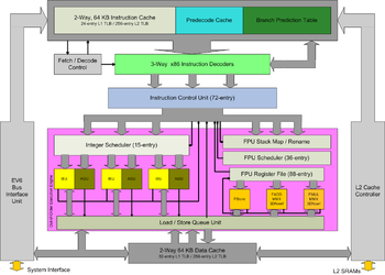
AMD Athlon is the brand name applied to a series of x86-compatible microprocessors designed and manufactured by Advance Micro Devices.[5] The K7 design team was led by Dirk Meyer, who had previously worked as a lead engineer at DEC on multiple Alpha microprocessors.[1] Wrote the Los Angeles Times on October 5, 1999: "AMD has historically trailed Intel’s fastest processors, but has overtaken the industry leader with the new Athlon.Analysts say the Athlon, which will be used by Compaq, IBM and other manufacturers in their most powerful PCs, is significantly faster than Intel’s flagship Pentium III, which runs at a top speed of 600MHz.By working with Motorola, AMD had been able to refine copper interconnect manufacturing about one year before Intel, with the revised process permitting 180-nanometer processor production.The accompanying die-shrink resulted in lower power consumption, permitting AMD to increase Athlon clock speeds to the 1 GHz range.[11] By the summer of 2000, AMD was shipping Athlons at high volume, and the chips were being used in systems by Gateway, Hewlett-Packard, and Fujitsu Siemens Computers among others.[2] This iteration of Athlon used AMD's Zen-based Raven Ridge core, which in turn had debuted in Ryzen with Radeon graphics processors.[18] With the release, AMD began using the Athlon brand name to refer to "low-cost, high-volume products", in a situation similar to both Intel's Celeron and Pentium Gold.[27] SRAM cache designs at the time were incapable of keeping up with the Athlon's clock scalability, resulting in compromised CPU performance in some computers.[25] The Slot-A Athlons were the first multiplier-locked CPUs from AMD, preventing users from setting their own desired clock speed.[29] AMD designed the CPU with more robust x86 instruction decoding capabilities than that of K6, to enhance its ability to keep more data in-flight at once.[30] Like the AMD K5 and K6, the Athlon dynamically buffered internal micro-instructions at runtime resulting from parallel x86 instruction decoding.[citation needed] AMD ended its long-time handicap with floating point x87 performance by designing a super-pipelined, out-of-order, triple-issue floating-point unit (FPU).[25] The Athlon XP was marketed using a performance rating (PR) system comparing it to the Thunderbird predecessor core.Palomino also had enhanced K7's TLB architecture and included a hardware data prefetch mechanism to take better advantage of memory bandwidth.[25] A revised Thoroughbred core, Thoroughbred-B, added a ninth "metal layer" to the eight-layered Thoroughbred-A, offering improvement in headroom over the A and making it popular for overclocking.[46] By this point with the Barton, the four-year-old Athlon EV6 bus architecture had scaled to its limit and required a redesign to exceed the performance of newer Intel processors.[49] Notably, the 2500+ Barton with 11× multiplier was effectively identical to the 3200+ part other than the FSB speed it was binned for, meaning that seamless overclocking was possible more often than not.Early Thortons could be restored to the full Barton specification with the enabling of the other half of the L2 cache from a slight CPU surface modification, but the result was not always reliable.


Athlon SportsAth.Lonx86-compatiblemicroprocessorsAdvance Micro DevicesAthlon 64Athlon IIAccelerated Processing UnitSocket AM1Socket AM4Zen (microarchitecture)Radeon GraphicsJerry SandersAMD K6Motorolacopper-based semiconductor technologyDirk MeyerCompaqNexGenVinod DhamLos Angeles TimesPentium III180-nanometerGatewayHewlett-PackardFujitsu Siemens ComputersPhenomSempronAthlon 64 X2Athlon X2Athlon IIRadeonRyzen 3CeleronIntel PentiumRadeon VegaIntel UHD GraphicsList of AMD Athlon processorsclock rateTechnology nodeInstruction setSlot ASocket ASocket 563K6-IIIAthlon XPSlot ASlot 1motherboardback-side busfront-side buscomplementary metal–oxide–semiconductoraluminium interconnectCPU cache2-way associativeHarvard architectureout-of-orderAlpha 21264double data ratefloating pointpipelinedfloating-point unit3DNow!extended MMXIntel SSEpin-grid arraySocket AAm386DX-40DresdenList of AMD Athlon XP processorsMicroarchitectureAthlon 64Windows XPperformance ratingprefetch3DNow! ProfessionalHardwareZonesteppingsdie shrinkPentium 4on-chip memory controllerHyperTransportceramicinterposerorganic pin grid arrayPowerNow!Cool'n'Quietsocket 563multiplieroverclockersList of AMD Athlon 64 processorsreleased in 2007 and 2009List of AMD Athlon X2 processorsAthlon 64 X2List of AMD Athlon II processorsExcavator microarchitectureSocket AM4x86-64AMD APURyzen 5L3 cacheL2 cachesupercomputersBeowulf clusterTokyo Institute of TechnologyTOP500Ohio Supercomputer CenterUniversity of ToledoRutgers UniversityGFLOPSList of AMD Athlon processorsList of AMD Duron processorsList of AMD Phenom processorsList of AMD Opteron processorsList of AMD Sempron processorsThe Wall Street JournalThe RegisterIEEE Journal of Solid-State CircuitsBibcodeKeith DiefendorffMicroprocessor Reportbinary meaningsAnandtechAMD processorsProcessorsAthlon