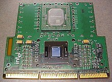
Pentium II
[6] This larger package was a compromise allowing Intel to separate the secondary cache from the processor while still keeping it on a closely coupled back-side bus.The improved 16-bit performance and MMX support made it a better choice for consumer-level operating systems, such as Windows 9x, and multimedia applications.[13][14] The original Klamath Pentium II microprocessor (Intel product code 80522) ran at 233, 266, and 300 MHz and was produced in a 0.35 μm process.[15] These CPUs had a 66 MHz front-side bus and were initially used on motherboards equipped with the aging Intel 440FX Natoma chipset designed for the Pentium Pro.[16] Pentium II-based systems using the Intel 440LX Balboa chipset widely popularized SDRAM (which was to replace EDO RAM and was already introduced with 430VX), and the AGP graphics bus.The Deschutes core Pentium II (80523), which debuted at 333 MHz in January 1998, was produced with a 0.25 μm process and has a significantly lower power draw.The 333 MHz variant was the final Pentium II CPU that used the older 66 MT/s front-side bus; all subsequent Deschutes-core models used a 100 MT/s FSB.[15] The Deschutes core introduced FXSAVE and FXRSTOR instructions for fast FPU context save and restore.Late Pentium IIs also marked the switch to flip-chip based packaging with direct heatsink contact to the die, as opposed to traditional bonding.Later, in 1999, the 0.25; 0.18 (400 MHz) μm Dixon core with 256 KB of on-die full speed cache was produced for the mobile market.


clock rateTechnology nodeMicroarchitectureInstruction setTransistorsSlot 1Mini-CartridgeμPGA1PentiumPentium ProPentium MMXPentium IIICeleronPentium 4SECC cartridgemicroprocessorsMMX instruction setL2 cacheSlot 2symmetric multiprocessingCPU socketdaughterboardheatsinkback-side bus16-bitIntel MMXWindows 9xtag RAMfront-side busIntel 440LXEDO RAMOverclockersflip-chipPentium II XeonworkstationsserversSocket 8ProcesssemiconductorList of Intel Pentium II microprocessorsIntel Celeronarchive.todayc't – magazin für computertechnikHeise VerlagWayback MachinePentium (original)Intel processorsProcessorsItaniumMicroarchitecturesChipsets32-bitP6 variant (Pentium M)P6 variant (Enhanced Pentium M)NetBurstx86-6464-bitPenrynNehalemWestmereSandy BridgeIvy BridgeHaswellBroadwellSkylakeCannon LakeSunny CoveCypress CoveWillow CoveGolden CoveBonnellSaltwellSilvermontGoldmontGoldmont PlusTremontGracemont80C18780387SX80387DXRapidCADOverDriveA100/A110Original i586Dual-CoreP6-basedNetBurst-basedCore-basedTolapaiNehalem-basedSandy Bridge-basedIvy Bridge-basedHaswell-basedBroadwell-basedSkylake-basediAPX 432StrongARMXScaleTick–tock modelProcess–architecture–optimization modelIntel GPUsIntel HD, UHD, and Iris GraphicsStratixCodenamesLarrabee