Negative-feedback amplifier
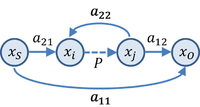
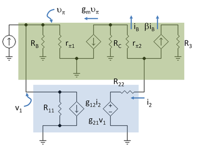
Negative feedback trades gain for higher linearity (reducing distortion) and can provide other benefits.[4] Harold Stephen Black independently invented the negative-feedback amplifier while he was a passenger on the Lackawanna Ferry (from Hoboken Terminal to Manhattan) on his way to work at Bell Laboratories (located in Manhattan instead of New Jersey in 1927) on August 2, 1927[5] (US Patent 2,102,671,[6] issued in 1937).On a blank space in his copy of The New York Times,[7] he recorded the diagram found in Figure 1 and the equations derived below.Black later wrote: "One reason for the delay was that the concept was so contrary to established beliefs that the Patent Office initially did not believe it would work.For an operational amplifier, two resistors forming a voltage divider may be used for the feedback network to set β between 0 and 1.This network may be modified using reactive elements like capacitors or inductors to (a) give frequency-dependent closed-loop gain as in equalization/tone-control circuits or (b) construct oscillators.The result of subtraction applied to the amplifier input is Substituting for V′in in the first expression, Rearranging: Then the gain of the amplifier with feedback, called the closed-loop gain, AFB is given by If AOL ≫ 1, then AFB ≈ 1 / β, and the effective amplification (or closed-loop gain) AFB is set by the feedback constant β, and hence set by the feedback network, usually a simple reproducible network, thus making linearizing and stabilizing the amplification characteristics straightforward.If there are conditions where β AOL = −1, the amplifier has infinite amplification – it has become an oscillator, and the system is unstable.The combination L = −β AOL appears commonly in feedback analysis and is called the loop gain.When feedback is present, the so-called closed-loop gain, as shown in the formula of the previous section, becomes The last expression shows that the feedback amplifier still has a single-time-constant behavior, but the corner frequency is now increased by the improvement factor (1 + β A0), and the gain at zero frequency has dropped by exactly the same factor.[24][25][26] Commenting upon the signal-flow approach, Choma says:[27] Following up on this suggestion, a signal-flow graph for a negative-feedback amplifier is shown in the figure, which is patterned after one by D'Amico et al..[23] Following these authors, the notation is as follows: Using this graph, these authors derive the generalized gain expression in terms of the control parameter P that defines the controlled source relationship xj = Pxi: Combining these results, the gain is given by To employ this formula, one has to identify a critical controlled source for the particular amplifier circuit in hand.Here the two-port method used in most textbooks is presented,[31][32][33][34] using the circuit treated in the article on asymptotic gain model.That is, the input side of the two-port is a dependent current source controlled by the voltage at the top of resistor R2.The next task is to select the g-parameters so that the two-port of Figure 4 is electrically equivalent to the L-section made up of R2 and Rf.The next step is to draw the small-signal schematic for the amplifier with the two-port in place using the hybrid-pi model for the transistors.The result for the open-loop current gain AOL is: In the classical approach to feedback, the feedforward represented by the VCVS (that is, g21 v1) is neglected.To explain these effects of feedback upon impedances, first a digression on how two-port theory approaches resistance determination, and then its application to the amplifier at hand.A broader conclusion, independent of the quantitative details, is that feedback can be used to increase or to decrease the input and output impedance.The improvement factor that reduces the gain, namely ( 1 + βFB AOL), directly decides the effect of feedback upon the input and output resistances of the amplifier.A reminder: AOL is the loaded open loop gain found above, as modified by the resistors of the feedback network.Therefore, feedback has no effect on the output impedance, which remains simply RC2 as seen by the load resistor RL in Figure 3.Figure 7 shows the small-signal schematic with the main amplifier and the feedback two-port in shaded boxes.Figure 7 shows the interesting fact that the main amplifier does not satisfy the port conditions at its input and output unless the ground connections are chosen to make that happen.This current is divided three ways: to the feedback network, to the bias resistor RB and to the base resistance of the input transistor rπ.This artificiality is a weakness of this approach: the port conditions are needed to justify the method, but the circuit really is unaffected by how currents are traded among ground connections.[39] The improvement factors (1 + βFB AOL) for determining input and output impedance might not work.As a consequence, when the port conditions are in doubt, at least two approaches are possible to establish whether improvement factors are accurate: either simulate an example using Spice and compare results with use of an improvement factor, or calculate the impedance using a test source and compare results.[34] Simple amplifiers like the common emitter configuration have primarily low-order distortion, such as the 2nd and 3rd harmonics.[46][47] However, as the amount of negative feedback is increased further, all harmonics are reduced, returning the distortion to inaudibility, and then improving it beyond the original zero-feedback stage (provided the system is strictly stable).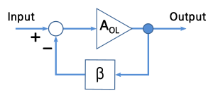


electronicamplifiernegative feedbackstep responseattenuatingfilteringvacuum tubesbipolar transistorsMOS transistorsnonlineardistortionoscillationNyquist stability criterionHarry NyquistBell LaboratoriesimpedanceHarold Stephen Blackrepeateroperational amplifiercapacitorsinductorsNyquist plotloop gainOpen-loop gaincutoffcorner frequencygain–bandwidth tradeoffringingovershoottwo-port networkssignal-flow graphsignal-flow analysisreturn-ratio methodasymptotic gain modeltwo-port networktwo-portstwo-portvoltage followerhybrid-pi modelvoltage divisionKirchhoff's voltage lawNortonThévenintwo-port feedback networksOhm's lawcurrent divisionport conditionssignal flow graphRosenstark methodBlackman's theoremtransconductancetransresistancecommon emitterharmonic seriesmaskinghuman hearing systemaudiophileBode plotCommon collectorExtra element theoremFrequency compensationMiller theoremOperational amplifier applicationsPhase marginPole splittingReturn ratioAnalog DevicesCiteSeerXBibcodeWayback Machine