Hybrid integrated circuit
Hybrid circuits could be encapsulated in epoxy, as shown in the photo, or in military and space applications, a lid was soldered onto the package.[3] In military and space applications, numerous integrated circuits, transistors and diodes, in their die form, would be placed on either a ceramic or beryllium substrate.Multi-layer thick film is a technique for further improvements in integration using a screen printed insulating dielectric to ensure connections between layers are made only where required.Once the hybrid circuit is fully populated with components, fine tuning prior to final test may be achieved by active laser trimming.Capacitors and semiconductors were in the form of LID (Leadless Inverted Devices) soldered to the surface by selectively heating the substrate from the underside.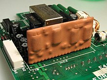


Telephone hybridMixed-signal integrated circuitprinted circuit boardelectronic circuitsemiconductortransistorsdiodesmonolithic ICsresistorsinductorstransformerscapacitorsPrinted wiring boardMIL-PRF-38534Integrated circuitMulti-chip modulesolderedThick film technologylaser trimmingDEC J-11three-dimensionalIBM System/360hybrid coilsintegrated circuitsvacuum tubesaudio amplifierChip on boardSystem in a packageMonolithic microwave integrated circuitSolid Logic TechnologyPrinted Electronic CircuitDigital electronicsComponentsTransistorResistorInductorCapacitorPrinted electronicsFlip-flopMemory cellCombinational logicSequential logicLogic gateBoolean circuitThree-dimensional integrated circuitEmitter-coupled logicErasable programmable logic deviceMacrocell arrayProgrammable logic arrayProgrammable logic deviceProgrammable Array LogicGeneric Array LogicComplex programmable logic deviceField-programmable gate arrayField-programmable object arrayApplication-specific integrated circuitTensor Processing UnitDigital signalBoolean algebraLogic synthesisLogic in computer scienceComputer architectureDigital signal processingCircuit minimizationSwitching circuit theoryGate equivalentDesignPlace and routePlacementRoutingTransaction-level modelingRegister-transfer levelHardware description languageHigh-level synthesisFormal equivalence checkingSynchronous logicAsynchronous logicFinite-state machineHierarchical state machineComputer hardwareHardware accelerationDigital audioDigital photographyDigital videocinematographytelevisionElectronic literatureMetastabilityRunt pulse